

WELCOME
TO THE EUROPEAN
PROJECT GIBON WEB SITE
TO THE EUROPEAN
PROJECT GIBON WEB SITE


Large bandwidth photodiodes of the waveguide type can be integrated within Photonic Integrated Circuits owing to their waveguide structure; they can also be integrated with electronic preamplifiers owing to the Semi-Insulating InP substrate on which they are grown. In GIBON, such photodiodes have first been optimized for their operation at 100Gbit/s (pin mesa size, steering from the the input waveguide, input taper, electrical termination
)..
Passivated waveguide-integrated photodetector with spot-size converter, termination resistor and biasing network. For 5x20 µm2 sized, AR-coated photodiodes, responsivity >0.6 A/W, bandwidth > 100GHz and polarization loss dispersion < 0.25 dB were achieved
WP3 Receiver Integration (Lead partner: HHI)
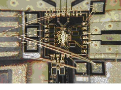
HEMT transconductance for various gate width & SEM view of the 130nm gate (upper left & right); view of the pigtailed pin-TWA OEIC & packaged photoreceiver (lower left & right)
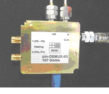
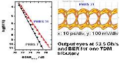
Co-packaging the photodetector chip and the DEMUX chip in one module housing with very short bonding wires (upper left and right) allows recovery of the tributaries without any error floor for the longest sequences, illustrating the good performance of the devices and the quality of the integration process (lower graph and eye diagram). Worth noting are the record sensitivities of +1.7 dBm and + 4.7 dBm at 107 Gbit/s for PRBS of 27-1 and 231-1 respectively.
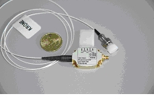
pin-TWA OEIC ( OptoElectronic Integrated Circuit) photoreceivers were designed and fabricated, associating a waveguide type photodiode and a 5-stage travelling wave preamplifier made in the InP HEMT technology. Specific developments were necessary to produce working devices.
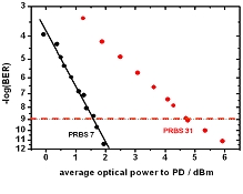
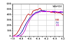
By combining a high-speed photodiode and a decision Flip-Flop in a same package, a high sensitivity demultiplexing receiver was assembled. The InP-based 1.55 µm high-speed photodiode is of the waveguide-integrated type exceeding 105 GHz bandwidth. The demultiplexing circuit is a Decision Flip-Flop fabricated in the InP Double heterojunction process. Co-packaging the two devices in a same module greatly reduces electrical losses due to separate housings and interconnections, by roughly 6 dB. World-leading sensitivity can then be obtained (see figure below). A same approach was followed with the co-packaging of a pin-TWA OEIC and decision Flip-Flop; preliminary characterization has shown full functionality, and a 4.7 dBm sensitivity at 10-9 BER
- Tuning the HEMT process, usually performed on the HEMT layer stack directly grown onto the SI substrate, to fit the situation of having the MOVPE grown SI waveguide layers in between
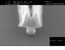
- Defining a process suited to the non planar OEIC, in particular for the e-beam writing of the short gate ( 100 nm length).
- Owing to the high transconductance obtained (750mS/mm intrinsic gain before BCB passivation) the gain provided by the TWA amounted to 4.7 dB.
- Owing to the high transconductance obtained (750mS/mm intrinsic gain before BCB passivation) the gain provided by the TWA amounted to 4.7 dB.